|
|
|
|
Selecting the right hardware for Reverse Time Migration |
Similar to GPGPUs, FPGAs are usually classified as streaming computation devices. However, the actual `streaming' mechanism differs significantly between GPGPUs and FPGAs. While a GPGPU generally issues loads of identical threads to handle different data items (Single Instruction Multiple Data), an FPGA pushes one data item through loads of different operations (Single Data Multiple Instruction). In a fully-pipelined FPGA design, you may even have different data items processed for different operations at different pipe stages (Multiple Data Multiple Instructions).
Before diving into the technical details of FPGA implementations, this section provides a general picture of the streaming architecture of FPGA computation compared to the classical Von Neumann architecture.
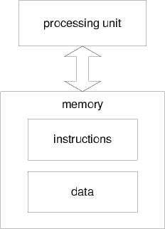
Figure 5 shows a classical Von Neumann architecture containing two major parts, the processing unit and the memory. The memory stores both the data and instructions. To execute each instruction, the processing unit loads the first instruction in the sequence and the related data from the memory, performs the corresponding arithmetic or logic operations, and stores the data back into the memory.
In contrast to the Von Neumann, FPGAs take a streaming approach to perform computation.
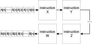
Figure 6 shows how as the data items are pushed in and out as sequential streams, the instructions are mapped into programmable circuit units along the path from the input ports to output ports. Therefore, instead of fetching instructions and data back and forth from the memory, the computation gets performed as the data streams flow through the circuit units in one pass.
|
|---|
|
von-neumann
Figure 5. The classical Von Neumann architecture.[NR] |
|
|
|
stream
Figure 6. FPGA streaming architecture.[NR] |
|
|---|---|
|
|
The performance of an FPGA streaming design relates to two key factors: one is how fast we can clock the pipeline, i.e. the throughput of the FPGA circuit; the other one is how fast we can push the data in and out, i.e. the bandwidth between the FPGA and the outside data.
To achieve a high computation throughput, the FPGA designs are generally fully-pipelined, with registers storing intermediate computation results. With pipelining, the throughput of the entire design is no longer determined by the latency of entire pass. Instead, the throughput is determined by the largest latency among circuit parts separated by registers. Therefore, for current commercial FPGAs, as long as the FPGA has enough registers to break the large latency into small separated parts, the computation throughput of the design can always be optimized to a level around the FPGA frequency. The pipelining in the design makes the FPGA's performance behavior quite different from conventional processors. In conventional processors, more mathematical operations consume more computation time. In FPGAs, more mathematical operations consume more hardware resources. While the latency from input to output port is increased, the throughput of the design remains the same. For applications like RTM that process a huge amount of data items, the long stream of input and output values hide the increase in latency.
Current commercial FPGAs contain three major categories of resources: reconfigurable logic; arithmetic units that can perform 18-bit by 25-bit multiplications; and Block RAMs that serve as distributed local storage units. On a current high end FPGA from Xilinx we can implement up to 1000 single-precision floating-point multipliers or 500 adders. Note that,if Moore's Law holds, these resources on the commercial FPGAs can get doubled every eighteen months.
|
|
|
|
Selecting the right hardware for Reverse Time Migration |