|
|
|
|
Accelerating 3D convolution using streaming architectures on FPGAs |
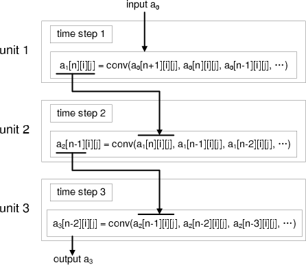
Instead of putting concurrent cores, another strategy is to process multiple time steps in one pass. Figure 4 shows the basic structure of a circuit that processes three time steps in one pass. The three units process three time steps separately with the output of each unit as the input of the next unit. The example in the figure uses a 3-by-3-by-3 `cube' stencil. In general, the computation of a wave-field data in slice ![]() requires the wave-field data in slices
requires the wave-field data in slices ![]() ,
, ![]() , and
, and ![]() in the previous time step. Therefore, when the unit
in the previous time step. Therefore, when the unit ![]() starts processing slice
starts processing slice ![]() , the unit
, the unit ![]() can start processing slice
can start processing slice ![]() . Meanwhile, unit
. Meanwhile, unit ![]() needs intermediate buffers to store the results for slices
needs intermediate buffers to store the results for slices ![]() and
and ![]() from unit
from unit ![]() .
.
|
multi-steps
Figure 4. Basic circuit structure for processing multiple time steps ( |
|
|---|---|
|
|
An advantage of processing multiple time steps over putting multiple stencil operators is that the performance will not be constrained by the memory bandwidth, as the unit for each time step is getting inputs from the previous time step, and does not consume the memory bandwidth of the FPGA.
However, on the data side, as we are doing a 3D blocking of the array, processing multiple time steps requires extra data items to start with. Given a convolution stencil with ![]() non-zero lags in each direction, to process
non-zero lags in each direction, to process ![]() time steps in one pass for a
time steps in one pass for a ![]() array, we need to start with an array of the size
array, we need to start with an array of the size
![]() . Considering doing 10 time steps for a 100x100 size, the data overhead is 44% for the `cube' and 156% for the `star'.
. Considering doing 10 time steps for a 100x100 size, the data overhead is 44% for the `cube' and 156% for the `star'.
Meanwhile, as the unit at each time step needs to store the results of the previous time step, this approach also increases the requirement for BRAM resources. Therefore, to increase the number of time steps, we need to reduce the blocking size, and thus increasing the cost of streaming overlapping data items and doing a larger number of streams.
Another advantage of this multiple-time-step architecture is that we can improve the order of time accuracy with relatively small costs. For example, for the unit ![]() in Figure 4, instead of only getting the previous wave-field data
in Figure 4, instead of only getting the previous wave-field data ![]() from unit
from unit ![]() , we can get in the wave-field data
, we can get in the wave-field data ![]() and
and ![]() from both units
from both units ![]() and
and ![]() to achieve 4th order in time accuracy. The cost for improving the time order is the extra buffer to store the wave-field data from unit
to achieve 4th order in time accuracy. The cost for improving the time order is the extra buffer to store the wave-field data from unit ![]() and the increased number of adders and multipliers.
and the increased number of adders and multipliers.
Figure 5 shows the estimated performance for FPGA convolution designs that process multiple time steps in one pass. The `star', the 2nd and 4th order `cube' are compared here. For this approach, the `cube' stencil shows a much better performance than the `star' stencil due to its smaller requirement for BRAM resources (`star' needs to buffer six slices for the convolution operation, while `cube' only needs to buffer two). Due to the constraint of logic slices, the FPGA can fit eight time steps for the `star', six and five steps for the 2nd and 4th order `cube'. The `star' gets its peak performance of 11x speedup with four time steps. After that, the performance becomes worse with more time steps. The 2nd order `cube' stencil increases all the way to 29x speedup with 6 time steps. The 4th order `cube' achieves 25x speedup with 5 time steps.
|
|
|
|
Accelerating 3D convolution using streaming architectures on FPGAs |